Nano-RF is a European project and the main concept is the development of CNT & graphene based advanced component technologies for the implementation of miniaturized electronic systems for 2020 and beyond wireless communications and radars.
The developed components and technologies developed during the project will be implemented in the following demonstrators:
- Reflect array antennae for wake vortex and weather radars
- Graphene receiver module
The demonstrators will exhibit the reconfigurability, systemability, integratability and manufacturability of the developed technologies and unify advanced More-than-Moore elements and Beyond-CMOS devices with existing technologies. It addresses "System Perspective" to support miniaturized electronic systems for 2020 and beyond.
This Nano-RF newsletter intends to present the latest progress obtained during first year of the project.
Design and Simulation activities
Existence of a negative imaginary conductivity leads to high inductive behavior compared to classical metals in microwave domain, leading to potential subharmonic resonances of CNT-based antennas. CNT-based antenna design is then reachable by parametric simulations directly on material characteristics through an arbitrary impedance surface definition. Input return losses and impedance, resonant frequency, frequency bandwidth in association with 3D radiation patterns are determined from S-parameters and far-field emission simulations result
First parametric simulations results have revealed an efficient radiation of a 750µm-length CNT bundle based quarter-wave dipole in the targeted working frequency range although the same topology implies a resonant frequency (lambda/2) at 100 GHz for a metallic wire of the same lenght.
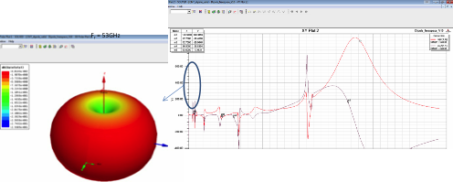
Figure 1 : Far field 3D gain radiation pattern at 53 GHz (a) a conductive tube with specific complex resistive surface (Zs = 0.001+j*0.01 Ohm.m2) – (b) Associated antenna input impedance as a function of frequency (red curve: real part – purple curve: imaginary part) - Dipole length:1.5 mm
- Graphene Antenna
We have started to design the graphene antenna which is a device not still reported and we have chosen a slot antenna in coplanar geometry depicted in the Figure 2 below:
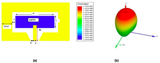
Figure 2 : (a) graphene coplanar antenna geometry (b) Radiation fields of the graphene coplanar antenna
Fabrication activities
- CNTs Growth
We have developed various recipes to grow CNTs in difference conditions and morphology for different applications in this project (RF switch, 3D interconnect and CNT FET). Both thermal chemical vapour deposition (TCVD) and plasma enhanced chemical vapour deposition (PECVD) method have been used to grow CNTs on different substrates. Different results are presented in Figure 3
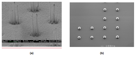 Figure 3 : (a) CNT vertically aligned obtained by PECVD for RF switch application; (b) CNT vertically aligned obtained by TCVD for 3D interconnect application
- CNTs devices fabrication and characterization
• 3D interconnect with CNTs
With a strong collaboration between SHT and Chalmers, we have grown high quality CNT bundles in through silicon vias (TSVs). The CNT bundles are firstly grown on Si surface and then densified by capillary force. The transferred structure is shown in Figure 4, which shows that the CNT bundle structure is retained after the transfer process.
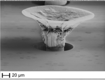
Figure 4 : Transferring densified CNT bundles into TSV structure
• CNTs antenna
UPMC in cooperation with IEMN as sub-contractor has set up an experimental probe test environment dedicated to vertical SW/MW CNT layer characterization with a 0.04-110 GHz working frequency. Homemade modeling tools taking into account coplanar multilayered configuration allowing microwave permittivity extraction were developed in order to qualify vertical MW CNT bundle material processed by technological process from TRT/SHT/Chalmers partners. Additional CNT electrical properties extraction, such as lineic inductance/capacitance and contact resistance with noble metals, are also under study to fulfill CNT-based nanodevices design tools.
First layouts of vertical CNT layer-based test samples for microwave material qualification from TRT/SHT/Chalmers process have been set up. First CNT-based quarter-wavelength grounded monopole layouts were designed with respect with technological process compatibility from TRT/SHT/ Chalmers partners. Microwave mounting tests have been fabricated in order to determine experimentally effective radiation of monopole MW CNT bundles of 1 x 1 mm3 (Figure 5) in a free space configuration. S-parameters and radiation patterns measurements are under work.
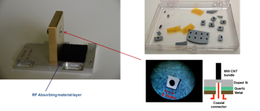
Figure 5 : First experimental microwave test structure configuration (c) of MW CNT bundle monopole on doped Si wafer (a) after wafer dicing/etching (TRT/MC2) and report on quartz substrate (b) implemented inside a protected microwave mounting with a 2,4 mm/50Ω coaxial access (with technical support of IEMN/MC2)
- Graphene Growth
There are several ways to obtain graphene material and we started to study the different graphene synthesis methods.
• Graphene CVD growth on metals
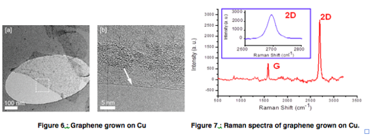
During this period, graphene is grown by CVD method. Using Cu as catalyst, high quality of graphene films with different number of layers are obtained, as shown in Figure 7 and Figure 8 below. SEM, TEM and Raman spectroscopy are used to evaluate the quality of the graphene material.
• SiC decomposition
Growth of graphene on silicon carbide has shown to be able to produce an outstanding quality over large area, for example demonstrated in spin transport, metrology and quantum hall physics. The surface rearranges and leaves a single layer of carbon atoms on the wafer. The silicon carbide substrates thereby may still influence the graphene. We have adapted a novel optical microscopy technique that allows to characterize the surfaces of graphene on silicon carbide over large area. This can confirm the uniformity and regular step features over large area Figure 8) and resolve both irregular features that may appear (inset Figure 8). This will be applied in the Nano-RF project to use uniform large area layers for further development.
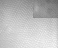
Figure 8 : Graphene on SiC
• Graphite ex-foliation
During the first year, different samples containing mono-crystalline graphene flakes produced using high resistivity silicon wafers (Figure 9) :
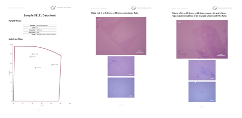
Figure 9 : graphene obtained by ex-foliation technic
Different samples provided by LiU (SiC decomposition), SHT/CHALMERS (CVD on metal) and Graphene Industries were analyzed by Raman spectroscopy. Raman characterization are presented on Figure 10:
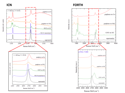
Figure 10 : Raman characterization from ICN compare with Forth
ICN has performed cross-plane thermal conductivity measurements of ZrO2 and HfO2 high-k dielectric thin films with thicknesses between 15 nm and 200 nm using the 3 omega method (Figure 11). The thermal conductivity was determined in a wide temperature range between 30 K and 300 K. The cross-plane thermal conductivity at room temperature was determined to 0.88 W/mK for ZrO2 and 0.65 W/mK for HfO2. The obtained results constitute important input parameters for the fabrication and optimization of the CNT and graphene based filters, FETs, switches, antennas, and interconnects.
Moreover, ICN has conducted extensive micro-Raman scattering studies on exfoliated and CVD grown graphene on different substrates. The measurements provide detailed information about the quality of the samples including strain, defect concentration, doping, and number of layers (Figure 11). Based on this information, the best fabrication technique is selected in order to ensure optimum conditions for the fabrication of graphene based RF devices.
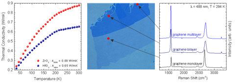
Figure 11 : (Left) Cross-plane thermal conductivity of high-k dielectric thin films ZrO2 and HfO2 measured by the 3 omega method in the temperature range from 30 K to 300 K, (middle) Optical microscopy image of exfoliated graphene with different number of layers, (right) local micro-Raman scattering spectra at the indicated positions of the graphene flakes.
- Graphene device fabrication and characterization
During the 1st year we have worked on graphene material characterization, graphene transfer, graphene patterning, graphene process modules development (ohmics, dielectrics, T gates for self align transistors) and graphene transistor fabrication.
However, the highlight, yet not totally confirmed, is the ohmic contact based on two materials and annealing which yielded very promising results (Table 1, Figure 12) :

Table 1: TLM results of contact X-Y on graphene with binary & Figure 12: TLM results comparison
CNRS – LAAS has developed an inverted process that enables the realization of a low loss high frequency complex yet flexible circuit based on graphene and/or CNT active device (Figure 13).
Measured high frequency performance surpasses that of high resistivity silicon in losses and provides a way to avoid graphene contamination during processing.
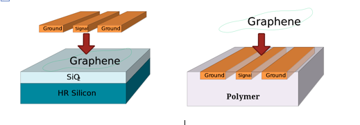
Figure 13: conventional (left) and inverted (right) processing concepts. The latter provides a low loss polymeric substrate and at the same time does not expose the sensitive graphene layer to many processing steps which reduces its contamination level.
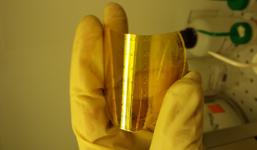
This concept is now being used to fabricate FET devices. An added bonus of this fabrication method is the fact that flexible circuits can be fabricated (Figure 14).
Nano-RF Publications
In the last 12 months the partners of the Nano-RF project published various results related to the project.• Publications
D.Dragoman and M.Dragoman, Geometrically induced rectification in two-dimensional ballistic nanodevices, J.Phys. D 46, 055306 (2013).
• Conference
International Conference on Spectroscopic Ellipsometry (ICSE-VI) Kyoto, Japan
Invited talk at RomPhysChem15, Bucharest, Romania
