The achievement of the proposed objectives can only be fulfilled through a well-coordinated effort. This undertaking involves tasks including system architecture, design and simulation of devices, material growth and characterization and fabrication of devices, test activities, system integration and, ultimately, technology transfer of the results achieved.
The Work Plan methodology is based on a top-down philosophy that employs efficiently both the broad expertise of the partners as well as their long-standing collaborative links. The goal is to devise novel technological “vehicles” in order to develop a new type of micro/nanosystems based on carbon nanotubes.
The organizational structure is shown in Figure below
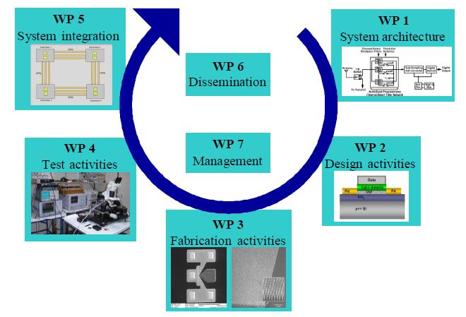
There are five interrelated work packages focussing on different aspects of the overall problem: specifications, design and simulation, fabrication, measurements and demonstration which are handled in work packages 1, 2, 3, 4, and 5 respectively. We combine experimental (WP3, 4, and 5) and modelling (WP2) skills to optimally tackle the problem: simulations and experiments are essential to narrow a rather large window of parameters from the chemistry, physics, and engineering perspective.
WP1 will deal with system specifications. We will identify and analyse all the parameters needed to design the CNT FET, switch, antenna, the graphene devices etc. It is of importance to have concrete values in order to properly design the devices. We will also review the applications for such nano T/R module for subsystems in wireless communication.
WP2 will be focused on the design and simulation activities. We will design and simulate the devices paying careful attention to the fact that these devices will have to work at very high frequencies (2-80 GHz).
WP3 will be devoted to the fabrication activities. First, we will study the material growth and characterization. We will study 2 CNT technologies: the controlled growth of dense perfectly aligned arrays of SWNTs by chemical vapor deposition (CVD), and the controlled growth of perfectly vertically aligned MWNTs by plasma enhanced CVD. The graphene will be deposited by Si/SiO2 using exfoliation techniques and possible using CVD or MBE growth. Full characterization (structural, electrical, thermal) will also be performed in this WP. Then, we will fabricate CNT FETs (power amplifier, low noise amplifier), the graphene low-noise amplifier, CNT NEMS (switch, filter, oscillator), and CNT based antennas and graphène multiplier and detector. In this WP we will also investigate different technological approaches that will allow for the system integration.
WP4 will gather the measurement and test activities. In this WP, we will test the devices fabricated in the WP above. For the CNT and graphene FET, a direct measurement setup will be built to fully characterize DC and AC properties. For the CNT NEMS, we will couple the switch with coplanar waveguides to characterize the switching of HF.
WP5 will target on system integration and test. The overall objective of this project is to demonstrate the feasibility of a nano T/R module based on CNT technology and graphene. It is thus of importance to think about the interconnectivity of our devices together. We will fabricate and test a nano T/R module based on the technologies above.
WP6 is devoted to dissemination of the results achieved towards scientific community as well as industry in the field of nanosystems. Identifiable means: website, workshops, e-newsletter, promotion via refereed journals and international conferences.
Finally, management activities are grouped into work package 7 (WP7). The management structure consists of: The general assembly, the executive board, the project coordinator, seven work package management teams, and seven work package leaders.


