Context of NANO-RF project
Micro/nanoelectronics are at the heart of the Information Society. When going from the micro towards the nanoscale, electronics still holds a lot of promises for smaller, more energy efficient and high frequency devices, but the scientific and technological developments in nanoelectronics have been uneven so far.
In the coming 10 years CMOS technology will reach the fundamental scaling limits of a charge-based switch at about 8 nm. Currently the 32 nm half pitch channel length is coming up while the 8 nm is anticipated perhaps around 2024. Mike Bryant, CTO of analyst firm. Future Horizons, says that there isn't a reliable silicon transistor based on 16 nanometre technology. Leakage and other problems will make silicon based transistors too unreliable as the process continues to shrink. He said that the properties of silicon limit the drive current to barely enough to drive the next gate.
To alleviate the silicon technology limits, numerous alternative approaches have been pursued (Si-Ge, III-V high mobility semiconductors) but it seems that the major breakthrough may come from materials exhibiting room temperature ballistic transport, namely carbon nanotubes (CNTs) and graphene. According to Nokia, carbon electronics represent a possible market of 1000M$ around 2025.
The potential of carbon electronics is currently acknowledged by The International Technology Roadmap for Semiconductors (ITRS), the ENIAC JTI and EPoSS. The International Technology Roadmap for Semiconductors (ITRS) [3], in which features sizes of integrated circuits will approach the 10 nm length scale, has motivated research in the electronic properties of nano-scale devices. Among other devices that have been investigated, CNTs are among the most recent and most promising with particular emphasis on their possible application in microwave and millimetre wave electronics.
CNTs have a wide field of applications and particularly in microwave and millimetre wave electronics. Indeed, the extraordinary mechanical and electrical properties of CNTs make them ideal candidates as building blocks for RF ICs. They can be metallic or semiconducting depending on their chirality. The high conductivity of single-wall (SWNT) metallic nanotubes or multi-wall nanotubes (MWNT) allow for designing simple actuation systems based on the direct electrostatic coupling with metallic gates. These properties make them particularly suitable for both basic building blocks of active components as well as electrical interconnects.
An overview of CNT properties is presented in Table 1
|
Parameter |
Values and units |
Observations |
|
Diameter/Length |
1 to tens of nm mm to mm and even cm |
The best electron emitters ever known |
|
Current density |
> 109 A/cm2 |
Highest current density of any material |
|
Thermal conductivity |
6,600 W/mK |
More thermally conductive than most crystals |
|
Young modulus |
1 TPa |
Among the stiffest materials |
|
Mobility |
10,000-50,000 cm2V–1s–1 |
Simulations: mobilities beyond 100,000 cm2V–1s–1 |
|
Mean free path (ballistic transport) |
0.3-1.2 μm in semiconducting CNT 1-3 μm in metallic CNT |
Measured at room temperature At least three times larger than in semiconducting heterostructures |
|
Conductance in ballistic transport |
G = 2´(2e2/h) = 155 mS |
1/G = 6.5 kW |
Table 1
Graphene has emerged as a promising material for electronics in the last years. It is chemically and thermally one of the most robust materials available. Furthermore it has proven potential for ultra-high frequency electronics. In less than 6 years from the material discovery by A. Geim and K. Novoselov, and despite the remaining technological issues still under heavy development, scientist have managed to provide proof of concept active devices (FET’s) operating at frequency comparable to the state of the art. Especially for wireless applications, an important factor is that graphene microwave devices can be easily accommodated to the standard 50 W impedance. Additionally, the nonlinear behaviour of the I-V dependence of graphene contacted with metals can be used to multiply or detect RF signals. Moreover graphene growth is rapidly progressing from a purely scientific field into the world of applications. An overview of graphene properties is presented in the table below.
|
Parameter |
Values and units |
Observations |
|
Mobility |
40 000 cm2V–1s–1 |
At room temperature (intrinsic mobility 200 000 cm2V–1s–1 in suspended structures) |
|
Mean free path (ballistic transport) |
200- 400 nm |
At room temperature |
|
Fermi velocity |
c/300=1000000 m/s |
At room temperature |
|
Thermal conductivity |
5000 W/mK |
Among the stiffest materials |
|
Mobility |
10,000-50,000 cm2V–1s–1 |
Better thermal conductivity than in most crystals |
|
Young modulus |
1.5 TPa |
Ten times greater than in steel |
Based on these properties, the development of CNT and graphene based advanced component technologies for the implementation of More than Moore and Beyond CMOS miniaturised electronic systems for 2020 and beyond wireless communications, promises significant breakthroughs.
The coordinator (TRT) of NANO-RF is the main multidisciplinary research unit of the THALES group, one of the major world players in civilian & professional electronics. TAS is N°1 in Europe and N° 3 worldwide in onboard equipment, sub-systems and systems both for civil and military aerospace markets. One key area for their products is transmit and receive front-end systems for numerous applications like radars for which long term solutions are continuously sought after. Their current technology is GaAs based while it will be replaced in the near future with GaN based one. However, the long term beyond 2020 envisaged solution is based on carbon electronics (CNTs, Graphene, NEMS)
Concept of NANO-RF project
Transmit/Receive (T/R) modules are key building blocks for modern communication arrays.
The concept of NANO-RF is to develop a new approach for future generation of T/R modules by using CNT and graphene technologies leading to a revolutionary new “nano T/R module” working at very high frequencies (up to 80 GHz).
The application spectrum is very broad: from satellite, aeronautics, and mobile communications to automotive radars.
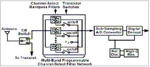
The T/R module’s most critical components are: a power amplifier (PA), a low noise amplifier (LNA) respectively within transmit and receive paths, a high isolation with low insertion loss back end switch component (SPDT), and finally a radiating element (antenna). Moreover, there are oscillators, mixers and filters (Figure 1). A recent trend in smart systems is the integration in a three-dimensional (3D) manner, i.e. stacking integrated circuits and components vertically in order to meet the challenges of performance enhancement, miniaturisation, power consumption, and thermal management. A key element in 3D integration is the vertical interconnection bridging the stacked components. NANO-RF will explore the possibilities of using CNTs as the interconnection material and assess their performance and reliability.
The NANO-RF concept will be realised through the following:
- To use CNT based field effect transistors (FETs) as building blocks for PA and LNA. The high mobility of CNTs (105 cm2/Vs) makes CNT FETs attractive for this kind of application and their high-saturated electron velocity (> 108 cm/s) leads to projected operation in the 2-80 GHz range1. Moreover, thanks to the nonlinearities of the FET and the nanotube, the CNT FET lends itself to be used as a mixer.
- To use CNT based NEMS switches as a building block for the high isolation/low insertion loss RF switch single pole double throw (SPDT). In fact CNT NEMS microwave switches display higher performances than their microscale counterparts, i.e., RF MEMS. In this way, the low loss and high isolation gained via RF MEMS are preserved but the switching time is drastically reduced up to tens of ns or lower. Such high-speed devices are a must for future communication smart systems2. CNT NEMS can also be used as voltage controlled oscillators and CN varactor as band pass filters.
- To fabricate of capacitive CNT NEMS switches for power application.
- To use CN based nano-antennas as a building block for the radiating elements. An advantage of CNT antennas is that the CNT can serve as an excellent impedance matching circuit to go from free space to high-impedance devices. In fact, CNT can be grown with length up to 1cm 3, which is comparable in length to the wavelength of microwaves in free space.
- To use CNTs as vertical interconnects in 3D integrated systems. The potential benefits include higher current carrying capacity, better high temperature stability, and better thermomechanical reliability.
- To fabricate a graphene FET transistor having performances beyond the state of the art and to use it to fabricate a LNA
- To use the nonlinear electrical properties of graphene to design and fabricate a microwave mixer and a detector
- To use graphene as a substrate for antennas and to fabricate an integrated receiver on graphene at the wafer level
- To achieve integration of these technologies to conceive, fabricate and test a nano T/R module.
- To use nano T/R module in parallel to achieve a max power requested by ENDUSERS.
Using CNT and graphene based devices as the main building blocks for the components of a T/R module will bring about a totally new concept towards its miniaturization. In fact, each of these components will benefit from several properties of the CNTs and graphene as well as from the high-density of integration between them.

Figure 1: T/R module’s most critical components
The CNT technology will address components such as switches, oscillators, filters, mixers, LNAs and PAs based on FET, and antennas while graphene will address the following components: LNAs (targeting ultra-low noise), mixers (acting as oscillator), detectors and antenna.
Technical work of NANO-RF
Technical work of NANO-RF project can be listed as follows:
- Achievement of design and technological/fabrication rules of nanosystems based on CNTs and graphene for microwave applications (2-80 GHz range). This requires that the individual devices be designed with high-frequency operation in mind, minimizing contact resistances and parasitic capacitances, and interfacing the CNT and graphène components optimally to the rest of the system, both structurally and electrically.
- (i) Demonstration of a CNT FET working at high frequencies (2-80 GHz) based on perfectly aligned, horizontal to the substrate, arrays of linear single-walled carbon nanotubes (SWNTs). Demonstration of a top- gate graphene transistor working in the same range of frequency.[especially for 10 Ghz]
(ii) Demonstration of a CNT FET mixer.
(iii) Demonstration of a CNT NEMS switch of microwave signals (2-80 GHz) based on array of vertically aligned, perpendicular to the substrate or horizontally aligned, multi-walled carbon nanotubes (MWNTs).
(iv) Demonstration of an oscillator based on CNT resonator or CNT varactor.
(v) Demonstration of a RF filter based on CNT arrays.
(vi) Demonstration of a CNT antenna based on individual/array of horizontal SWNT with lengths in the mm-cm range working in the 2 to 80 GHz range.
(vii) Demonstration of a graphene multiplier and detector able to demodulated RF signals.
(viii) Demonstration of a microwave graphene FET beyond the state of the art and a LNA based on it
(ix) Demonstration of a microwave antenna on graphene substrate
(x) Demonstration of a graphene receiver at the wafer level.
- System integration and test of a nano T/R module based on the above technologies. Solutions to highly integrated smart systems with CNTs as interconnects will also be studied. The focus will be on using CNTs as vertical interconnects in 3D integrated systems.
To achieve such ambitious objectives we plan to extensively study the CNT and graphène technology through:
(i) growth of vertically and/or laterally, individual and/or arrays of CNTs in precise locations on silicon wafers
(ii) deposition of large graphene flakes on Si substrates compatible with CMOS technology
(iii) design and simulation of CNT and graphene devices and ICs aiming towards reproducibility
(iv) fabrication modules for CNT and graphene based devices aiming towards manufacturability and realiability
(v) integration of CNTs as vertical interconnects with high conductivity, high reliability, and good compatibility with other technologies. Design/simulation activities will be also of importance, as the devices will be operated at very high frequencies in the 2-80 GHz range.
At the end of the project, we will unveil the potential of the developed technologies through the realization of 2 demonstrators (1 on CNTs and 1 on graphene).


